





We publish what we learn on the line: which tolerances a fabricator can actually hold, how a stackup choice changes impedance, and where assembly yield is lost. Every article is written by the engineering team that runs the process, and each one states the standards and numbers behind the advice.
What we cover
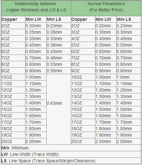
- Fabrication — layer count, copper weight, minimum trace and spacing, vias, plating and surface finish.
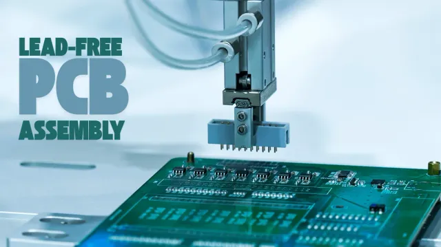
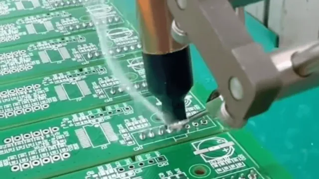
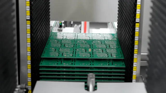
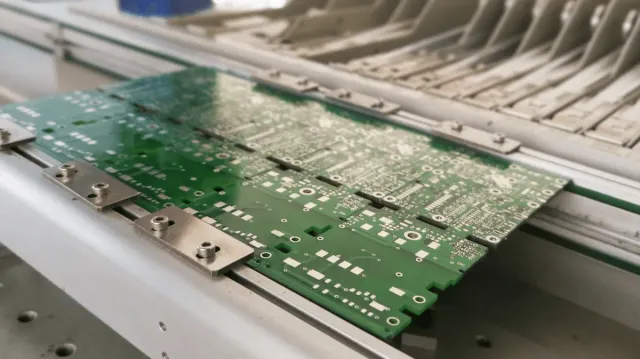
- Assembly — stencil and paste printing, placement, reflow profiles, inspection, test coverage and rework.
- Materials — FR-4 and high-Tg laminates, polyimide, ceramic, metal-core and high-frequency materials.
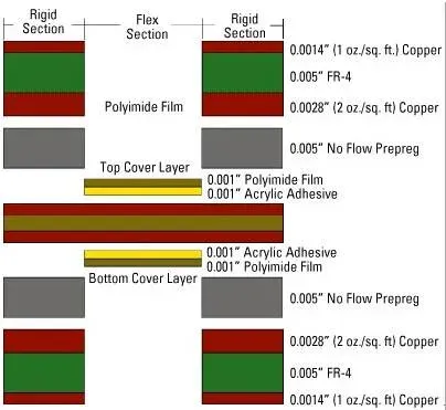
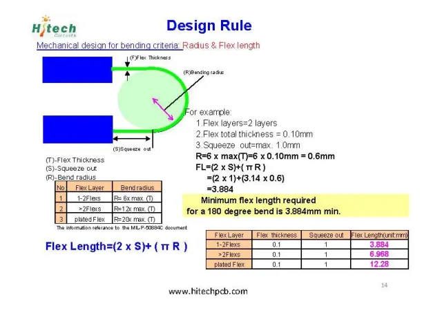
- Flex & HDI — flex and rigid-flex stackups, stiffeners, microvia rules and high-density routing.
- Sourcing — BOM review, approved manufacturers, obsolete-part handling, cost drivers and incoming inspection.
- Industry — automotive and LED applications, plus notes from the trade shows we attend.
How to use these notes
Start with the process you are about to release. If a design rule is not covered, send the stackup or the Gerber set for a free engineering review before tooling starts; we answer with the specific limit that applies to your board rather than a generic table.
If you need a quotation, include the layer count, material, surface finish, copper weight, board size, quantity and test requirements — that is enough for a same-day first pass.