
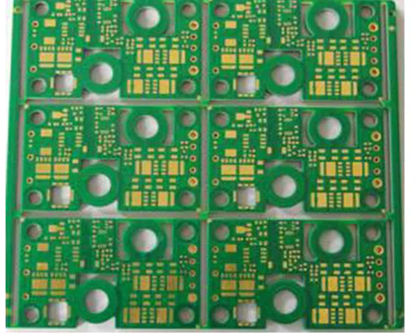
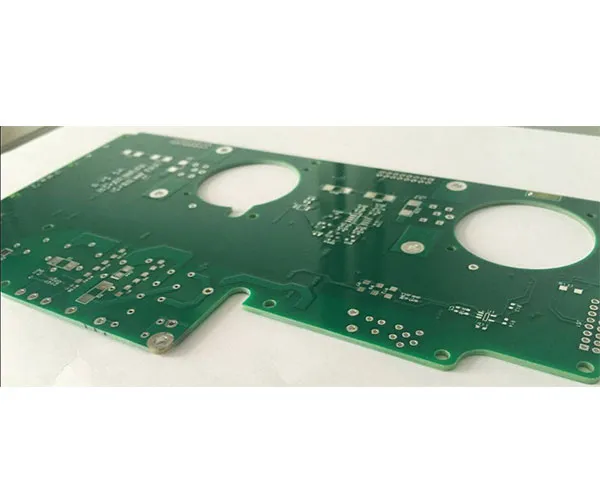
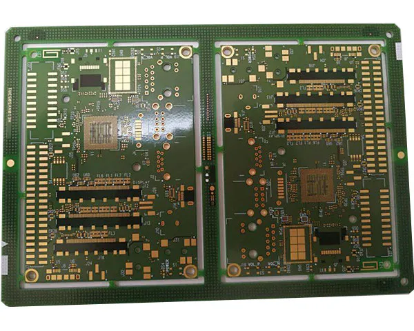
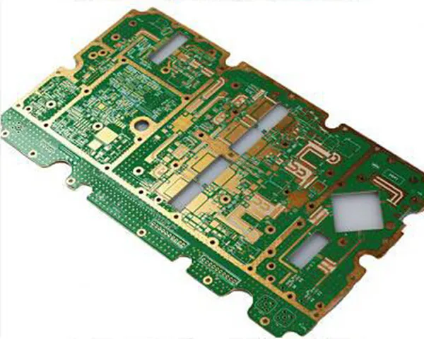
Printed circuit board manufacturing is the core of Hitech Circuits. Ten board families are produced in Shenzhen, and the limits behind them are published as numbers rather than adjectives: 1–38 rigid layers, 0.075 mm line and space, 0.1 mm laser-drilled vias, a 15:1 aspect ratio, outer-layer copper to 20 oz and panels up to 580 × 1900 mm.
What the plant fabricates
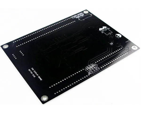
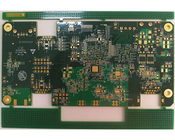
- Rigid and multilayer boards — 1–38 layers on FR-4, high-Tg FR-4, halogen-free laminate, CEM1 and FR-1, from a small prototype panel to 580 × 1900 mm production tooling.
- HDI boards — 1+N+1, 2+N+2, 1+1+N+1+1 and 3+N+3 stack-ups with laser microvias and ELIC technology.
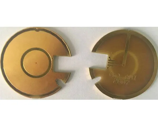
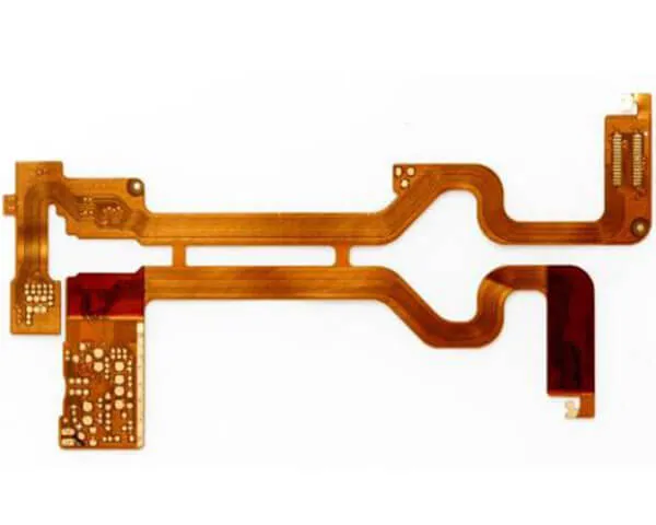
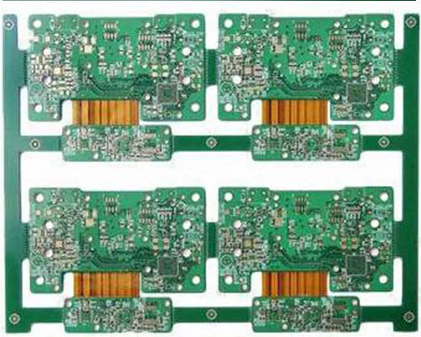
- Flexible and rigid-flex circuits — 1–12 layers on Kapton, PI and PET, bonded to FR-4 rigid sections, with 0.05 mm line and space and PI, PET, FR-4 or stainless-steel stiffeners.
- Metal-core boards — aluminium, copper and COB MCPCB constructions from 5 × 5 mm to 1900 × 480 mm, carrying 18–240 µm copper for LED, power and thermal designs.
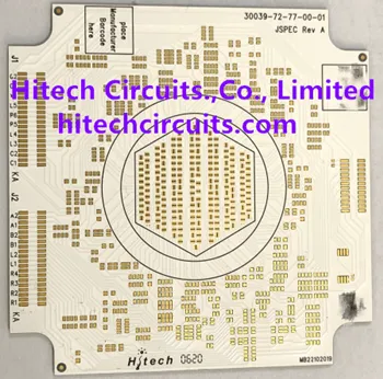
- Ceramic substrates — 96 % and 98 % alumina, aluminium nitride and beryllium oxide in thin-film, thick-film and direct copper bonded processes, for designs from −55 °C to 850 °C.
- Heavy-copper, high-frequency and quick-turn builds — up to 20 oz outer copper, Rogers, Arlon, Taconic and Nelco laminates with impedance held to ±10 %, and prototypes inside 1–3 days.
The details that decide a quotation
Four points settle most of the risk in a design: layer count and minimum line width, copper weight, impedance tolerance, and the documentation a customer's own approvals need. All of them are reviewed in DFM, DFA and DFT before quoting, so stack-up, panelisation or clearance problems surface while they are still cheap to fix.
Surface finish is fixed together with the stack-up — HASL, lead-free HASL, ENIG, ENEPIG, immersion silver, immersion tin, flash gold, golden finger, OSP, carbon ink and peelable mask are handled in-house — and the full process limits sit on the PCB manufacturing capabilities page.
When the boards continue into assembly and box build, the China PCB assembly page covers how fabrication, component sourcing and assembly are quoted as one order.
Bare board and assembly in one plant
Fabrication is only half the work. Four SMT lines place six million chips per day at 01005 and 0201 package sizes down to a 4 mil (0.1 mm) pitch, three DIP lines handle 1.6 million through-hole pieces per day, and BGA rework, re-balling and X-ray inspection cover the joints that cannot be seen. Cable and harness assembly and box build follow in the same building, so a product can ship as a built unit rather than as boards plus loose parts.
One quality system for every board type
ISO 9001:2015 is the base, with IATF 16949:2016 and ISO 13485:2016 layered on for automotive and medical work and ISO 14001 and ISO 45001 alongside them. Boards are fabricated to IPC-6012B and IPC-A-600H, UL recognised under file E354070 and RoHS compliant; the issued certificate scans are published on the certifications page.
How to start
Send the Gerber set or the BOM — or both — with the stack-up, quantity and target date. Prototypes come back in 1–3 days and medium-volume boards in 4–10 days, with stencils cut and delivered within four hours; mass production is scheduled once the BOM is released. The same board types are rebuilt for different markets, and the industries pages show what changes in each vertical.