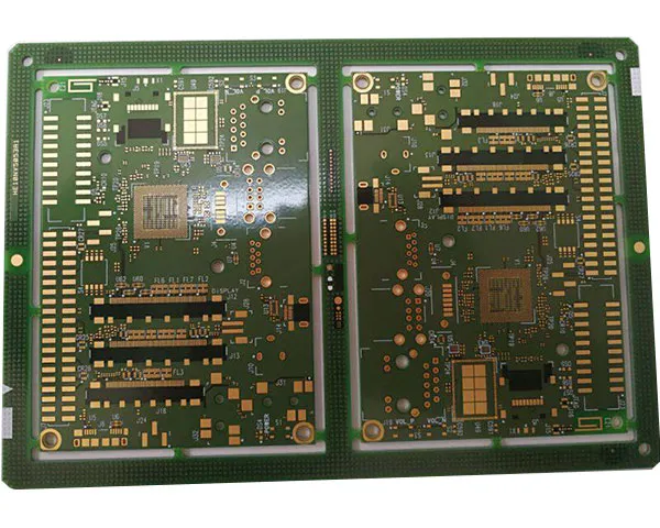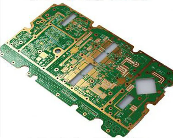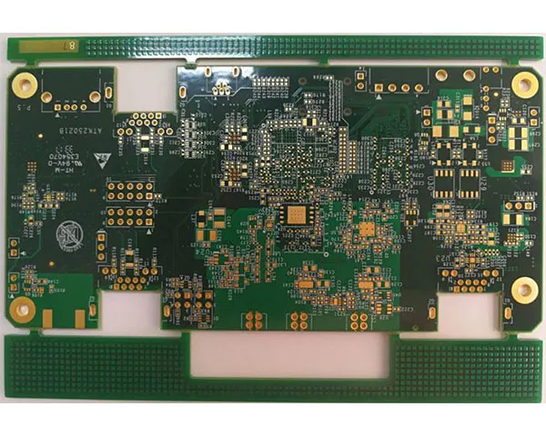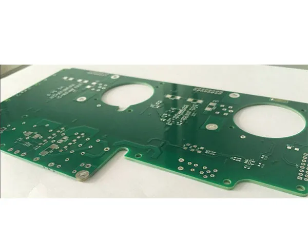
Etching a heavy copper layer is not the same process as etching a 1 oz layer, and the design rules that suit a signal board do not transfer to it. The differences show up first in line width and spacing, then in the clearances between conductors, in the thermal relief on every pad, and finally in whether the finished panel stays flat.
Line width and spacing against copper weight
One ounce of copper is about 35 µm, so a 3 oz layer is roughly three times the thickness of a standard layer and a 20 oz layer about twenty times. Etching removes copper from the side of every trace as well as from the surface, so a heavy layer loses more width while the gap beside it closes faster than the artwork shows. Minimum line width and spacing are therefore quoted against the copper weight, not as a single figure: 0.075 mm is available on fine-feature layers, while a heavy layer's limit is set by its thickness and agreed in the DFM review. The safest heavy-copper layouts use the copper to carry current in wide shapes and keep the fine geometry for the layers that can hold it.
Clearance and creepage
A thick conductor exposes a taller sidewall, and the voltage has to be held across that sidewall as well as across the surface distance between two traces. Creepage and clearance grow with copper weight, and the solder mask dam between two heavy traces has to stay wide enough to survive both the etch that forms it and the assembly temperatures it will later see. Where a heavy layer also carries high voltage, the clearance is set by the working voltage rather than by the process minimum — and that is a question for the design, not for the fabricator.
Thermal relief and assembly
A heavy pad holds heat. Thermal relief spokes are sized so the pad still reaches soldering temperature instead of acting as a heat sink, solder mask openings are widened to suit the thicker copper, and the via treatment — tenting, plugging or filling — is chosen so a heavy layer can still be processed reliably after lamination. Reflow profiles are extended for the extra thermal mass, which is one reason heavy copper designs are reviewed for assembly as well as for fabrication.
Copper balance and flatness
An unbalanced lay-up bows during lamination and again during reflow, so copper is balanced across the panel and through the thickness of the stack-up: heavy areas are mirrored where the design allows, and the remaining imbalance is handled in the process rather than left to the customer. Bow and twist are held to a maximum of 0.7 %, and a board that mixes a heavy power layer with a controlled-impedance signal layer keeps the 15:1 aspect ratio and the ±10 % impedance tolerance of the standard line.
Plated holes and panel size
Two dimensions are set by the plating process rather than by the artwork. In a heavy-copper build a plated through hole should finish at 0.3 mm or larger, with a 0.15 mm annular ring, and the same 0.3 mm floor applies to the smallest via. Wall copper in those barrels runs 20–25 µm in the normal case and 50–100 µm (2–5 oz) where the barrel itself has to carry current, which is why a heavy design needs a larger pad and a wider solder-mask opening than a signal board.
Panel size is a cost decision before it is a capability decision: 550 × 350 mm is the most economical panel for this process, and 550 × 500 mm can be built but costs noticeably more. The board itself may be larger — the published limit is 580 × 1900 mm — so where the design allows it, panelisation should follow the economical panel rather than the maximum.
Where the rules are checked
Every heavy copper enquiry goes through DFM, DFA and DFT before the quotation is fixed, so line width, clearances and panelisation are settled while the layout can still be changed. The board itself is described on the heavy copper PCB page, the process limits behind it on the capability page — including the power supply, motor drive, welding and plating equipment covered on the industrial control page.
Assembly and sourcing for the designs covered here are quoted from the same plant; the China PCB assembly page lists the process steps that follow fabrication.