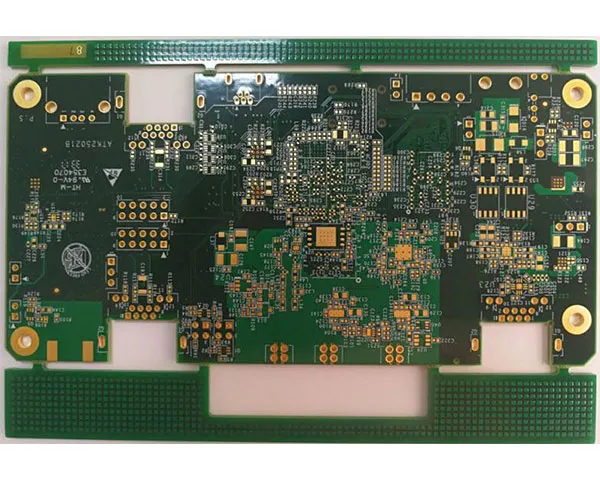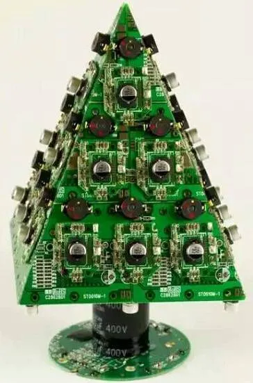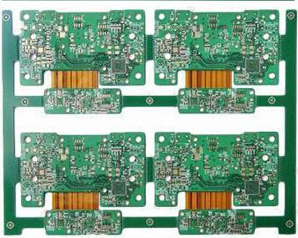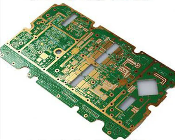
Above roughly 1 GHz a laminate stops behaving as a passive carrier. Dielectric loss arrives as attenuation, the dielectric constant sets the velocity of the signal and the length a stub may run, and moisture taken up from the air shifts both. A high-frequency board answers that with a material chosen for its electrical behaviour rather than its mechanical properties, and with a stack-up modelled before any copper is etched.
What changes above 1 GHz
- Loss — attenuation grows with frequency and with the dissipation factor of the laminate, so the material matters as much as the trace geometry.
- Dielectric constant — the trace width that gives a 50 Ω line depends on the dielectric constant and its tolerance, which is why the stack-up is fixed before routing.
- Moisture — absorbed water raises the effective dielectric constant and the loss, which is why the low-absorption laminates are used for equipment that works outdoors.
- Copper surface — at high frequency the current crowds into the surface of the conductor, so surface treatment and copper roughness are chosen with the finish, not after it.
- Mechanics — PTFE-based material is softer than FR-4, so drilling, hole treatment and panel support are adjusted for it rather than run on the standard recipe.
Materials and stock
Rogers, Arlon, Taconic and Nelco high-frequency laminates are held in stock, so a prototype does not wait on a material order; high-Tg FR-4 and halogen-free laminate cover the cases where the frequency is moderate and the budget is tighter. Boards are built from 1 to 38 layers up to 580 × 1900 mm, with 0.075 mm line and space on the fine-feature layers and 0.5–20 oz copper where a power section shares the stack-up.
Stack-up, impedance and assembly
Impedance is held to ±10 %: dielectric thickness, dielectric constant, copper weight and trace width are modelled together and then verified on the finished board. ENIG, immersion silver, immersion tin, flash gold, golden finger, HASL, lead-free HASL and OSP are all available, and mixed constructions are used where a digital section and an RF section share one board. Assembly runs in the same plant with four SMT lines at six million chips per day and X-ray inspection, so a populated RF module ships as one part.
Where high-frequency boards are used
Wireless and cellular infrastructure, satellite and radio equipment, radar and antenna modules, power amplifiers and low-noise amplifiers, and passive networks such as splitters, couplers, duplexers and filters. Automotive radar and telecommunications hardware are the volumes; where the temperature rather than the frequency is the hard requirement, a ceramic substrate takes over.
Getting a quotation
Send the Gerber set with the laminate, the stack-up, the target impedance and tolerance, the frequency range and quantity. Prototypes come back in 1–3 days and medium volume in 4–10 days; process limits are on the capability page and the issued certificates on the certifications page.
High-frequency boards that move into assembly are covered on the China PCB assembly page, including sourcing and box build.