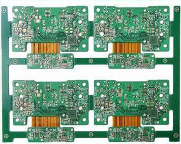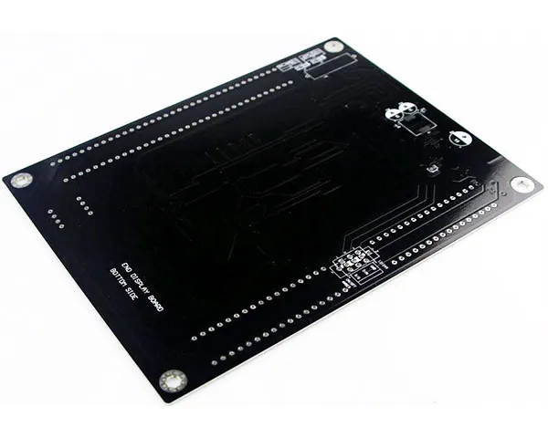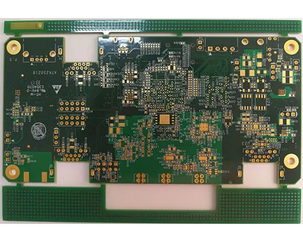
A multilayer PCB presses two or more inner conductor layers between insulating plies, then connects them to the outer layers with plated holes. The result is more routing in the same footprint, a solid reference plane under high-speed signals, and a shorter path between power and ground — which is why almost every product with a processor, a radio or a dense connector moves past two layers quickly.
Single-sided, double-sided and multilayer
- Single-sided — one copper layer, holes for through-hole parts only. Suitable for the simplest circuits and the lowest cost.
- Double-sided — copper on both faces, connected through plated holes, which carries the majority of small products.
- Multilayer — three or more conductor layers, inner layers processed before lamination and the outer layers afterwards. Hitech Circuits builds these from 4 to 38 layers, with 0.075 mm line and space and outer copper from 0.5 oz to 20 oz.
How the board is built
Inner layers are imaged, etched and inspected, then laminated under heat and pressure with the prepreg that sets the dielectric thickness between them. Drilling follows the stack-up: 0.15 mm mechanical holes and 0.1 mm laser holes with a 15:1 aspect ratio, copper plated to the inner layers, outer layers imaged and etched, then solder mask, surface finish and profile routing. Board thickness is held to ±8 % at 0.8 mm and above and ±10 % below that, with outline tolerance of ±0.10 mm and bow and twist inside 0.7 %.
Stack-up, impedance and materials
FR-4 covers most builds, with high-Tg FR-4 for boards that see repeated thermal cycling, halogen-free laminate where the customer's own approvals require it, and Rogers, Arlon, Taconic or Nelco where the signal has to survive at high frequency. Impedance is calculated from the stack-up and controlled to ±10 % — the same review fixes panelisation and copper balance so the finished panel does not bow. Where density rather than layer count is the constraint, microvia stack-ups from HDI boards are built on the same floor.
Where multilayer boards are used
Communications equipment, industrial control, GPS and satellite units, aerospace, computing, medical devices, military hardware — and the telecom and network hardware described on the telecommunications page. Boards for vehicles follow IATF 16949:2016 and medical boards follow ISO 13485:2016, both on top of the base ISO 9001:2015 system; fabrication runs to IPC-6012B and IPC-A-600H with UL recognition under file E354070.
Getting a quotation
Send the Gerber set, the stack-up or layer count, copper weight, impedance requirements and quantity. Prototypes come back in 1–3 days and medium volume in 4–10 days; the capability page lists the limits behind the quotation and the certifications page holds the issued certificates.
Multilayer boards that continue into assembly are quoted with component sourcing and box build on the China PCB assembly page.