The trade HDI makes
A conventional multilayer board buys routing space with layers. Every signal that cannot escape the surface gets a via through the whole board, and every added pair of layers costs laminate, drilling and lamination time.
An HDI board buys the same space with process cycles. A 0.1 mm laser microvia connects only the two layers it needs to, so the through-hole that would have blocked every layer below disappears. What replaces it is sequential lamination: the core is built first, then layers are added around the microvias, one cycle at a time.
So the comparison is not "old technology against new". It is two ways of paying for density — in material, or in process.
Where conventional still wins
Below a certain pin density, a through-hole multilayer is simply cheaper. Standard drills, one lamination cycle, no via filling, no laser, and a design rule set that every fabricator and assembly house knows. Boards with 0.5 mm and coarser pitch, modest layer counts and room for wide escape routing rarely justify HDI.
The case for HDI appears when one of these is true:
- a fine-pitch BGA or CSP has to escape on the outer layers,
- the connector field cannot be routed without via-in-pad,
- the layer count needed by through-hole routing pushes the board past what the thickness or cost allows,
- the product needs the same function in less board area.
Counting the cycles
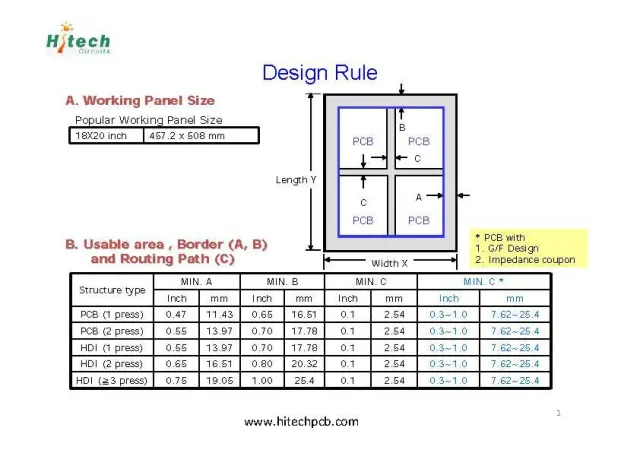
Hitech Circuits builds 1+N+1, 2+N+2, 1+1+N+1+1 and 3+N+3 stack-ups, up to ELIC where every layer is interconnected by microvias, with 0.1 mm laser vias and 0.075 mm line and space. Core boards can go to 38 layers, and through-holes keep a 15:1 aspect ratio.
Each cycle is a decision. A single 1+N+1 cycle handles most fine-pitch escapes; a stacked 2+N+2 or 3+N+3 build is chosen when the package needs several successive layers of connection. ELIC is the most capable and the most expensive, and it is worth it only when the routing cannot be closed any other way.
A decision list
- Count the nets that cannot escape on the surface layers. If there are few, stay conventional.
- Check whether another pair of layers closes the routing. If yes, compare that cost against an HDI cycle.
- If via-in-pad is required under a BGA, HDI is effectively already decided — through-holes cannot be filled and capped under pads at that pitch.
- Choose the smallest number of sequential cycles that closes the design.
The product page lists the HDI stack-ups and process limits, and the capability page covers the through-hole and microvia ranges in one place. If both options are plausible, send the stack-up intent and the drill table and ask for a comparison — we build HDI and conventional multilayer on the same floor.