Menu
Blog

NEPCON JAPAN 2026, Tokyo

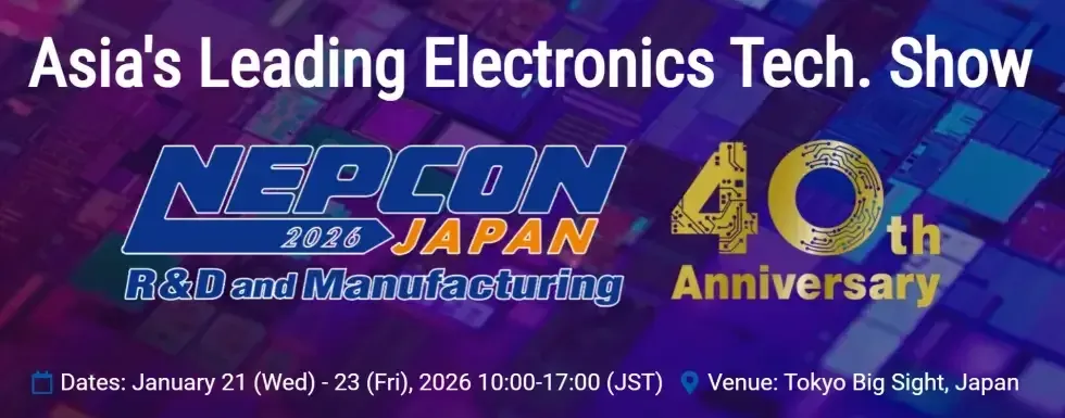
We exhibited at the 40th NEPCON JAPAN at Tokyo Big Sight, 21–23 January 2026, on booth E26-16 in East Hall 6.

Hitech Circuits Engineering Desk

Shenzhen, China · PCB fabrication and assembly

2 min read

Published:

Last updated:

Technical review: Process figures checked against our published capability sheet. View capability sheet

Hitech Circuits at the NEPCON JAPAN 2026, Meet Us at E26-16 at East Hall 6

About the event

NEPCON JAPAN is the electronics R&D, manufacturing and packaging exhibition held at Tokyo Big Sight. The 2026 edition was the 40th, and it draws engineers from automotive, consumer electronics and semiconductor equipment companies alongside component and material suppliers.

For a board supplier, the value is not footfall. It is the density of technical questions: a stack-up that has to survive 150 °C, a ceramic substrate replacing a metal core, a rigid-flex section that has to fold into a housing.

What we showed

  • Heavy copper — 0.5–20 oz outer, 0.5–10 oz inner, for converters, motor drives and welding equipment.
  • Ceramic — 96 % and 98 % alumina, aluminium nitride and DCB, for high-temperature and RF work.
  • Rigid-flex and flex — up to 12 layers on Kapton and polyimide, with PI, PET, FR-4 or stainless-steel stiffeners.
  • HDI — 1+N+1 to 3+N+3 and ELIC, with 0.1 mm laser microvias.
  • PCBA — assembled boards from the same site, so fabrication and assembly are one conversation.

Follow-up

If you visited the booth, write to sales@hitechcircuits.com with the project details and mention NEPCON JAPAN 2026. Sending the stack-up and the drill table in advance lets the review start before the next call.

The process limits are on the capability page; the board families are described on the PCB manufacturing page, and the assembly side on the PCBA manufacturing page.
Technical Specifications

Event
40th NEPCON JAPAN, Tokyo Big Sight
Dates
21–23 January 2026
Booth
E26-16, East Hall 6
Focus
heavy copper, ceramic, rigid-flex and HDI boards, plus PCBA

Frequently Asked Questions

  • What did Hitech Circuits show at NEPCON JAPAN 2026?

    The boards that carry the process limits rather than the catalogue: heavy copper PCBs up to 20 oz outer and 10 oz inner, ceramic substrates on alumina and aluminium nitride, rigid-flex builds up to 12 layers, and HDI stack-ups from 1+N+1 to 3+N+3. Assembled boards ran alongside them, so a visitor could see the same part before and after SMT.

  • Can a project discussed at the show still be quoted?

    Yes. Send the Gerber set, stack-up, BOM and quantity to sales@hitechcircuits.com and mention NEPCON JAPAN 2026. A BOM quotation comes back within 24 hours of a complete package, and prototypes run in 1–3 days, so the timing of the show has no effect on the lead time.

  • Why exhibit in Tokyo?

    Japan is one of the densest concentrations of automotive, industrial and semiconductor equipment engineering in the world, and those are exactly the applications where heavy copper, ceramic and HDI boards matter. A show is the fastest way to see which of those requirements are moving into the next generation of products.

← Blog

Related engineering notes

Request a customer quote

Free engineering review and quote for PCB manufacturing, PCB assembly, component sourcing and box build.