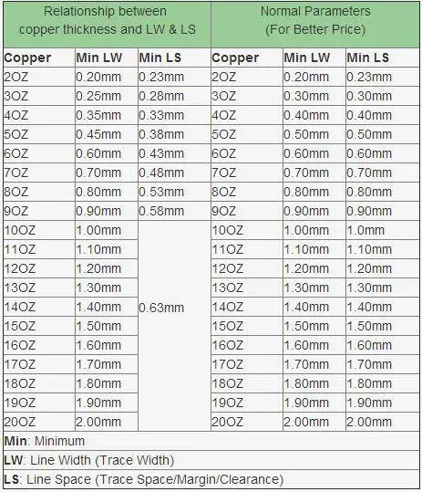
The rule set was written for thin foil
Most PCB design guides assume 0.5–1 oz copper. Reset the trace width to 0.075 mm, the hole to 0.2 mm and the annular ring to a comfortable 0.15 mm, and the layout passes every check in the DRC. On a heavy layer the same numbers mean something different: they describe features that the etch and the plating bath cannot produce together.
A heavy copper layout is therefore checked against three things, in this order.
Check one: feature size follows weight
Etching is not directional. Copper is removed from the top of the trace and from the side at once, so the finished width is narrower than the artwork and the gap beside it is wider. On 35 µm foil that undercut is a small fraction of the trace; on a 105 µm layer it is a large one, and on a 700 µm layer the effect decides what can exist at all.
Hence the split in the rules: 0.075 mm line and space stays available on fine-feature layers, while a heavy layer's minimum is set by its copper weight and confirmed in DFM. The most reliable heavy copper layouts use wide shapes to carry current and leave the fine geometry to the layers that can hold it.
Check two: holes, rings and aspect
A heavy layer is thick enough to change how a hole is drilled, plated and cleaned. The plant minimum is 0.15 mm mechanically or 0.1 mm with a laser, and the aspect ratio is 15:1: a barrel deeper than fifteen times its diameter cannot be plated evenly.
Two design habits follow. Keep vias out of heavy layers where a thinner layer can take them, and check the annular ring against the copper weight rather than the drill table, because the heavier the layer, the more of the pad the etch takes.
Check three: balance, panel and flatness
Heavy copper on one side of a stack-up makes the panel bow during lamination and again during reflow. Copper is mirrored across the lay-up where the design allows, and the remainder is handled in the process — but a layout that puts all the copper on the top layers leaves the fabricator little to work with.
Panel size matters for the same reason. Boards inside 580 × 1900 mm plate and etch more evenly than arrays that fill the maximum, and bow and twist are held to 0.7 % against IPC-6012B and IPC-A-600H acceptance.
What to send for review
The Gerber set, the copper weight per layer, the current per net with the permitted temperature rise, the finished thickness and the quantity. With those five, DFM settles feature size, hole strategy and panelisation while the layout can still change — which is cheaper than discovering the limit after tooling. The rule set itself is on the heavy copper design guide, and the process limits on the capability page.


