Menu
Blog

Bow and Twist in PCB Manufacturing

A warped board fails at the printer, not at final inspection. Warp is designed in by unbalanced copper and heat.

Hitech Circuits Engineering Desk

Shenzhen, China · PCB fabrication and assembly

2 min read

Published:

Last updated:

Technical review: Process figures checked against our published capability sheet. View capability sheet

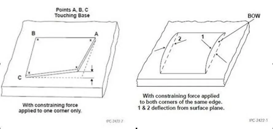
Bow & Twist Circuit Board Issue and Prevention

Causes

  • Copper imbalance between layers or between the two sides
  • Asymmetric dielectric build
  • Lamination and reflow thermal stress
  • Large unsupported areas and thin cores

Prevention

Balance copper by layer, keep the stackup symmetric around the centre, add thieving where a plane is missing, and agree the panel orientation with the fabricator.

Acceptance

Measure against the IPC limits for the board size and thickness. A board that passes at room temperature can still fail after reflow, so warpage is often checked after assembly simulation.


Technical Specifications

Acceptance
IPC-6012B / IPC-A-600H limits
Board thickness
0.1–6.0 mm
Layer count
1–38 layers

Frequently Asked Questions

  • What causes most bow and twist?

    Unbalanced copper distribution and asymmetric stackups. When one side has a large plane and the other has sparse routing, the two sides expand differently through lamination and reflow, and the board bends toward the stiffer side.

  • Does the finished board thickness fix the problem?

    Only partly. A thicker board resists bending, but if the copper is unbalanced the stress remains. The reliable fix is a symmetric stackup with copper thieving or a redesign of the plane distribution.

← Blog

Related engineering notes

Request a customer quote

Free engineering review and quote for PCB manufacturing, PCB assembly, component sourcing and box build.