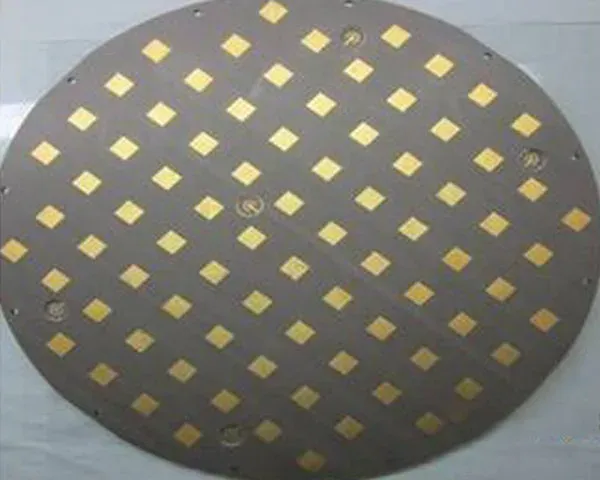
The layout is the circuit
Below a few hundred megahertz, a trace is a wire. Above that, it is a transmission line, and its impedance, its return path and its length are part of the electrical design. Ten rules cover most of the difference.
1. Put a reference plane under every RF trace
Continuous, unbroken, and on the layer directly beneath. A split plane forces the return current to detour, and the detour is the source of most mysterious RF behaviour.
2. Control the impedance, then verify it
Microstrip or stripline impedance is set by trace width, dielectric thickness and dielectric constant. The ±10 % tolerance is verified with a coupon on the panel, not assumed from the CAD stack.
3. Keep the RF path short and straight
Every millimetre of trace adds loss and every bend adds a discontinuity. Where a bend is unavoidable, use 45° chamfers or arcs rather than 90° corners.
4. Stitch the ground planes
Ground planes on different layers are tied together with vias placed close to every RF transition and along the board edge. Stitching keeps the planes at the same potential at RF, which is what makes them a reference.
5. Use via fences around sensitive traces
A row of ground vias on both sides of a sensitive trace creates a waveguide-like boundary that reduces coupling to neighbouring nets. The spacing has to be small relative to the wavelength, not to the trace width.
6. Design the launch, not just the trace
Where a connector or a cable meets the board, the geometry changes: pad width, ground return and solder fillet all affect impedance. A launch that is drawn as an afterthought produces a reflection that no amount of trace tuning fixes.
7. Keep digital and RF apart
Separate the RF section from switching supplies and digital routing, and keep the return currents separate until they meet at one defined point. A DC-DC converter next to an LNA is a design decision, not a layout accident.
8. Match lengths where it matters
Differential pairs and phased arrays need matched electrical length, and the match has to include the via transitions. On a hybrid stack, dielectric constant varies by layer, so matching on physical length alone can be wrong.
9. Decouple at the frequency you are fighting
A 100 nF capacitor does not decouple a 2.4 GHz supply transient by itself. The decoupling network is chosen for the band, placed close to the pin, and its return path goes straight to the ground plane.
10. Make the board measurable
Add test coupons for impedance, keep access to the RF chain for probing, and define the ground reference at the test point. A board that cannot be measured at the prototype stage will be debugged by swapping components.
Where material choice comes in
FR-4 is adequate for many sub-6 GHz designs, but its dissipation factor and dielectric constant vary with frequency, temperature and resin content. When the loss budget or phase stability demands more, RF laminates such as Rogers, Arlon, Taconic or Nelco are used — often in a hybrid stack with FR-4 in the core to control cost.
The material comparison is in the high-frequency material note; the process limits, including 0.075 mm features and ±10 % impedance, are on the capability page, and fine-pitch RF sections often combine with HDI.


