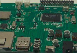
An IoT board is three designs on one substrate
A connected product has to do three things at once: transmit and receive a radio signal, run for months on a small battery, and measure something real through a sensor front end. Each of those puts a constraint on how the board is assembled — not just on how it is designed.
1. The radio needs a keepout
Antenna performance is decided by the geometry around it. Copper, ground planes, metal enclosures and batteries all change the tuning, and the effect is large enough that a board that passes conducted test can fail in the housing.
In assembly terms this means the keepout is treated as a real feature: no copper, no components, no coating and no label inside it. The area is marked on the assembly drawing, masked before any coating step, and checked at first article — because once the unit is potted or enclosed, nothing can be fixed.
2. The power budget is a process issue
Sleep current is measured in microamps, and at that level contamination matters. Flux residue on a high-impedance node, moisture inside a package, or a coating applied over an unclean board all create leakage paths that are invisible to a standard electrical test.
That is why a battery-powered product is worth cleaning and verifying before coating, rather than treating "no-clean" as an assumption. The measurement is part of functional test: current draw in each power state, not just the presence of the rails.
3. Thermal design in a sealed box
IoT devices are usually small and sealed, so heat has nowhere to go. A power amplifier, a regulator and a radio running together in a closed housing raise the local temperature well above ambient, and the sensor's accuracy drifts with it.
Assembly choices follow: thermal vias under the hot part, a metal stiffener or a heat spreader where the housing can conduct, and component placement that keeps the temperature sensor away from the regulator.
4. Coating, but selectively
Conformal coating protects a connected product from condensation, and it is one of the few post-assembly steps that changes the electrical behaviour of the board. The dielectric constant of the coating shifts the impedance of RF traces and detunes the antenna if it is applied inside the keepout.
So the coating is applied selectively: connectors, test points, pressure sensors and the antenna area are masked, and the rest of the board is covered to the specified thickness. The decision between coating and potting is covered in the coating comparison.
5. Test has to run the product
An IoT assembly can pass AOI, ICT and a power-on check and still fail the only test that matters: the radio link at the edge of range, the sensor reading under load, the current in sleep mode.
Functional test therefore runs the firmware, measures current in each state and exercises the radio, with a fixture that does not detune the antenna. Where the design includes RF traces on Rogers, Arlon, Taconic or Nelco laminate, impedance is held to ±10 % and verified through the stack-up.
What to send for a quote
The Gerber set, BOM, assembly drawing with the antenna keepout and coating mask, the firmware version for functional test, and the test specification for each power state. Prototypes come back in 1–3 days; 01005 and 0201 parts, mixed technology and selective coating all run on the same four SMT lines.
The process limits are on the PCBA manufacturing page; application context for connected products is on the consumer electronics and telecommunications pages.