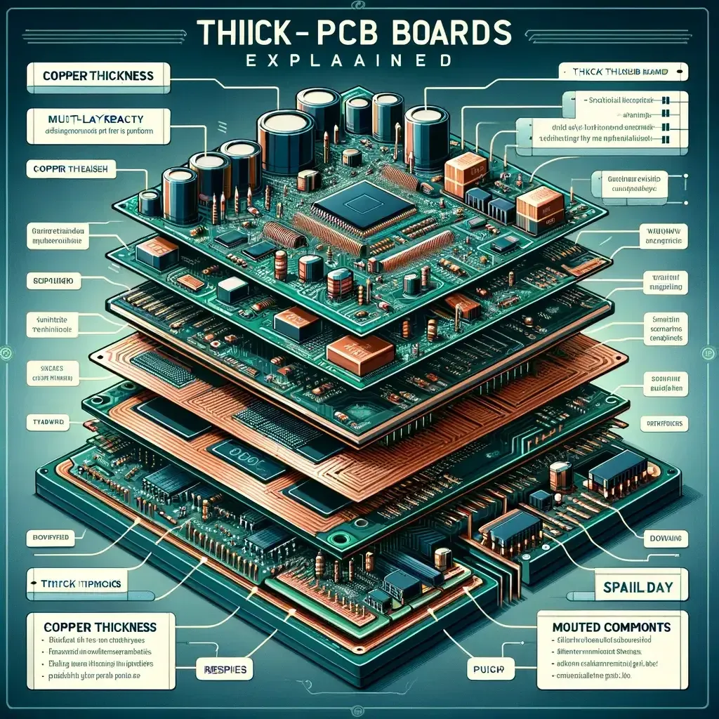
Why build a 6 mm board
Three reasons, usually together: a connector or edge-finger standard that fixes the thickness, a mechanical load the board has to carry, or a stack-up with many layers and heavy copper that only closes at that gauge.
Thickness is therefore a consequence of other decisions far more often than a goal in itself — which is why it is worth checking whether a stiffener or a thicker aluminium housing would do the same job for less money.
The aspect ratio sets the hole
The rule that matters: thickness ÷ finished hole diameter ≤ 15. At the top of the range:
| Board thickness | Smallest plated hole at 15:1 |
|---|---|
| 1.6 mm | 0.107 mm — so 0.15 mm mechanical is comfortable |
| 3.2 mm | 0.213 mm |
| 6.0 mm | 0.4 mm |
This is why a thick board and a fine-pitch BGA can be incompatible: the package needs small vias, and the thickness will not plate them. The usual resolution is a thinner board plus a stiffener, or a stacked construction.
Lamination and materials
A thick stack means more prepreg, more lamination cycles and more opportunity for registration error between layers. Two practical consequences:
- Registration tolerance accumulates. Each lamination cycle adds a shift, so annular ring and drill-to-copper margins are checked against the final stack, not the first pair.
- Resin flow has further to travel. Heavy copper and thick stacks need enough prepreg to fill the pattern, or the dielectric thins and impedance drifts.
Bow and twist stay at 0.7 % maximum, which is harder to hold as thickness and copper mass rise; a symmetric lay-up is the main lever.
Depanelisation
V-scoring works from 0.6 to 3.2 mm. Above that, the board is routed, and the choice of tab routing and breakout method has to be made with the thickness in mind — snapping a 6 mm tab by hand is not a plan.
Assembly
A thick board is a heat sink. Reflow profiles need a longer soak and a defined peak; selective and hand soldering need preheat from below. Press-fit connectors and edge fingers are checked against the finished thickness, and the fixture has to hold a board that weighs several times what a 1.6 mm panel does.
When thick is the wrong answer
If the requirement is stiffness or connector depth, a 1.6 mm board with a local stiffener, a metal carrier or a thicker housing is usually cheaper and easier to build than a uniform 6 mm laminate.
If the requirement is current, heavy copper on a thinner board may do the job: 20 oz on a 1.6 mm stack carries a lot of current without the aspect-ratio penalty.
The published limits are on the capability page, the multi-layer build in the process note, and the heavy copper options on the heavy copper PCB page.


