Menu
Blog

HDI PCB: Laser Vias and Stackups

HDI buys routing density with process steps. The decision is how many sequential laminations the design actually needs.

Hitech Circuits Engineering Desk

Shenzhen, China · PCB fabrication and assembly

2 min read

Published:

Last updated:

Technical review: Process figures checked against our published capability sheet. View capability sheet

High-Density Interconnect printed wiring board (HDI PWB)

The building blocks

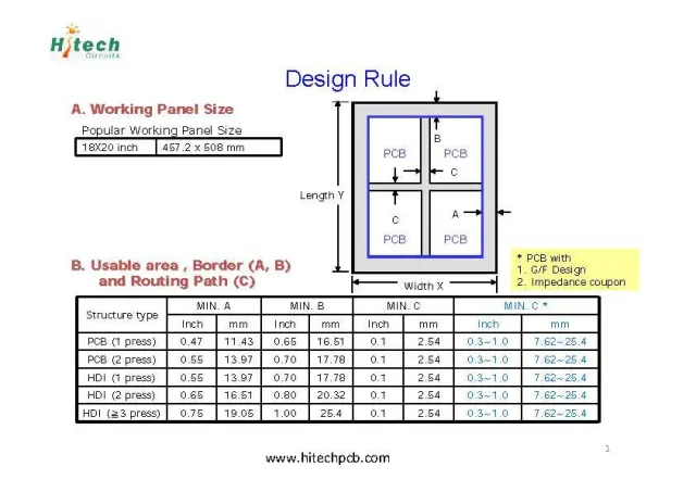
  • Microvias — laser-drilled, 0.1 mm on our lines, connecting adjacent layers.
  • Sequential lamination — the core is laminated first, then the outer layers are added around the microvias.
  • Via-in-pad and filled vias — allow components to be placed directly over the via.
  • Fine features — 0.075 mm trace and spacing on the outer layers.

How many cycles does the design need?

Start from the pin pitch. A fine-pitch BGA may escape on a single sequential cycle; denser packages need two or three. Each cycle adds lamination, drilling and plating steps, so the goal is the minimum that routes the board, not the smallest via the process can make.

What to send

Provide the stackup intent, the via types and the drill table, plus the impedance requirements if any. We build HDI and conventional multilayer on the same floor, up to 38 layers, with flex and rigid-flex up to 12 layers, so the review can compare both options before tooling.


Technical Specifications

Minimum laser via
0.1 mm
Minimum trace / spacing
0.075 mm / 0.075 mm
Layer count
1–38 layers; flex and rigid-flex up to 12

Frequently Asked Questions

  • What makes a board HDI rather than conventional multilayer?

    Microvias with a diameter below roughly 0.15 mm, produced by laser drilling and usually combined with sequential lamination and via-in-pad. The density comes from stacking these small vias between adjacent layers instead of drilling through the whole board.

  • Does HDI always reduce cost at high pin counts?

    It can, because fewer layers may be needed once microvias free up routing space. But each additional lamination cycle adds cost and yield risk, so the cheapest HDI stackup is the one with the fewest sequential cycles that still closes the routing.

← Blog

Related engineering notes

Request a customer quote

Free engineering review and quote for PCB manufacturing, PCB assembly, component sourcing and box build.