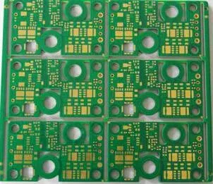
The definition
A printed circuit board is a laminated insulating substrate with patterned copper conductors on one or more layers, plated holes that connect those layers, a solder mask that keeps solder off everything except the pads, and a surface finish that keeps the exposed copper solderable.
Three things follow from that definition, and they matter commercially:
- It is a mechanical part. Thickness, flatness, edge quality and hole position are tolerances, not descriptions.
- It is passive. The board does not function on its own; it defines where current can go.
- It is specified, not described. A Gerber set without a stack-up and a finish is not a complete specification.
Anatomy
- Substrate — the laminate: FR-4, high-Tg FR-4, halogen-free, CEM1, FR-1, or a high-frequency material such as Rogers, Arlon, Taconic or Nelco.
- Copper — 1 oz is about 35 µm; the plant range runs from 0.5 to 20 oz on outer layers.
- Layers — from 1 to 38; the inner layers are imaged and etched before lamination, the outer layers after.
- Holes — plated through holes, blind and buried vias, and laser microvias from 0.1 mm.
- Solder mask and legend — the polymer cover and the printed reference markings.
- Finish — HASL, ENIG, immersion silver, immersion tin, OSP or carbon ink.
The families
| Family | What it is for | Typical limit |
|---|---|---|
| Single / double-sided | Simple circuits, low cost | 1–2 layers |
| Multilayer | Dense routing, controlled impedance | 1–38 layers here |
| HDI | Fine-pitch escape, microvias | 0.1 mm laser vias |
| Flex / rigid-flex | Movement or folding | up to 12 layers |
| Metal core | Heat spreading (LED, power) | 1–4 layers |
| Ceramic | High temperature, RF, high insulation | alumina, AlN |
What it is not
- Not a component. It carries components; it does not switch or amplify.
- Not a finished product. Even an assembly is a subassembly until the box build and final configuration are done.
- Not a commodity by default. Two boards with the same dimensions can differ by a factor of ten in price, depending on layer count, copper weight, feature size, finish and class.
From design to board
The sequence is short to describe and long to execute: design and stack-up, DFM review, inner-layer imaging and etch, lamination, drilling, plating, outer-layer imaging and etch, mask and legend, finish, routing and test. Each step has one job, and the order cannot be rearranged.
The process is described in the fabrication note; the industry vocabulary in the glossary; the difference between a board and an assembly in the PCB vs PCBA note. The published limits are on the capability page.


