Quality policy and objectives
The quality policy is set out in three lines: quality first, continuous improvement, customer satisfaction. It is turned into numbers that can be measured against a delivered order:
- Customer complaint rate: below 0.8 %
- Pass rate: above 98 %
- Defect rate: 500 ppm or less
- On-time delivery: 99.6 %
- Customer satisfaction: above 99 %
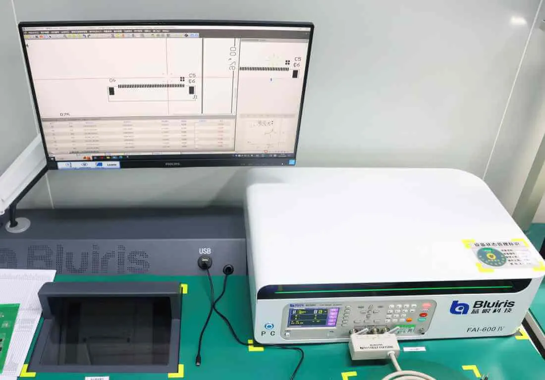
Those are the published objectives for the PCB and PCBA operations, not a claim about any single lot. On-time delivery is published as 99.6 % — the figure is the same on the capability, service and contact pages, so a buyer never reads two numbers for one metric. The inspection equipment below is what produces the data those objectives are measured from.
Certification
The quality system is certified for the markets the boards are sold into, so a customer can carry a Hitech Circuits board into a regulated product:
- ISO 9001:2015 — general quality management system
- IATF 16949:2016 — automotive programs, with PPAP documentation agreed at order entry
- ISO 13485:2016 — medical devices
- UL recognition under file E354070 — the boards themselves
- ISO 14001 and ISO 45001 — environment, and occupational health and safety
Issued copies of the certificates are on the certifications page. Material declarations follow the same route: RoHS compliance is screened on incoming material and finished boards, and REACH statements are issued from an SGS test report.
Checks during PCB fabrication
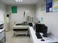
Bare-board work is verified against the drawing rather than by eye. The physics lab holds the dimensional and physical test stations, so measurements are taken in-house instead of being subcontracted:
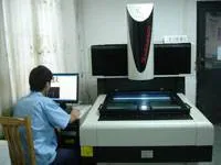
- 2D measurement — hole positions, pad dimensions, annular ring and board outline measured against the customer drawing
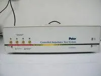
- Controlled impedance test system — impedance coupons from the production panel measured against the specified value, holding to the ±10 % tolerance published on the capability page
- Metallographic microscope — micro-sections of plated through holes and vias for plating thickness, barrel integrity and copper-to-resin adhesion
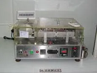
- Flexural proof tester — bending endurance on flex and rigid-flex samples to the bend requirement of the application
- RoHS screening instrument — element screening (lead, mercury, cadmium, hexavalent chromium and brominated flame retardants) on incoming material and finished boards


Checks during assembly
Assembly is inspected at each step, because a defect found after reflow costs more to correct than one found at printing:
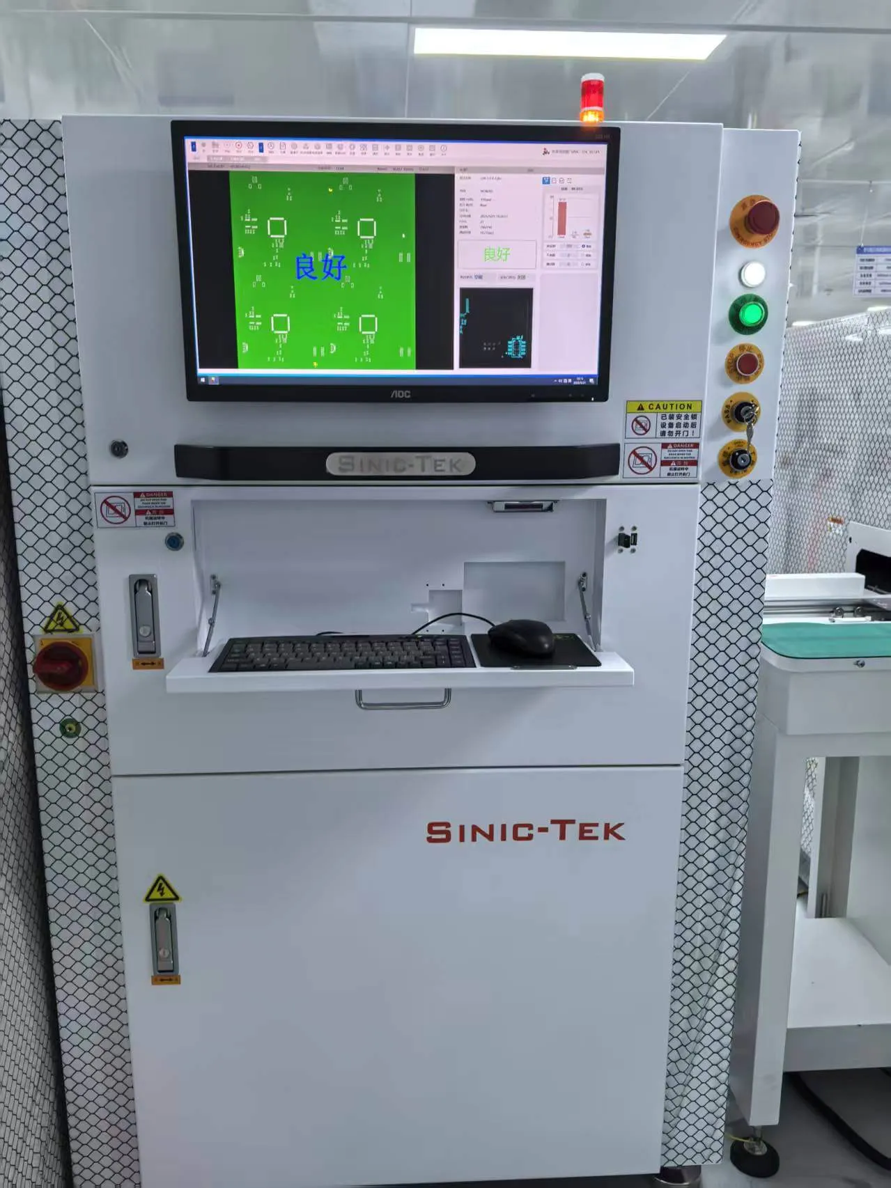
- Solder paste inspection (SPI) — paste volume, area and height are measured after printing, so a short or bridged deposit is wiped and reprinted before any component is placed.
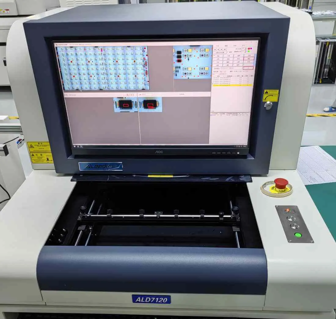
- Automated optical inspection (AOI) — after reflow, both sides of the board are compared against the inspection program, which flags missing, offset, reversed and poorly filleted joints.
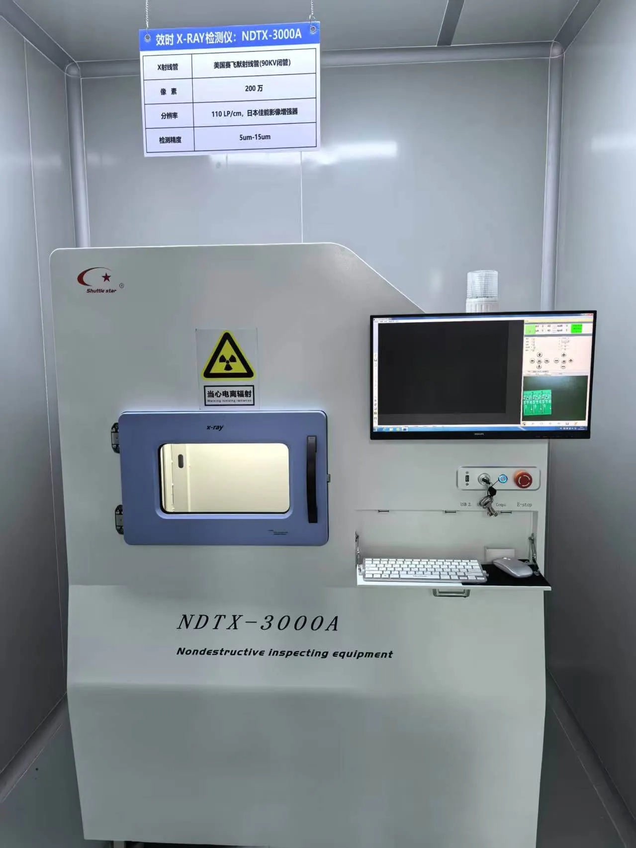
- X-ray inspection — joints hidden under BGA, QFN and QFP bodies, plus via and barrel quality, imaged at 110 LP/cm with 5–15 µm defect detection.
- First-article inspection — the first unit of a build is measured against the CAD data before the batch is released to run.
- Electrical test — in-circuit, flying probe and functional test against the customer test procedure; the options are described on the PCBA testing page.
Records that travel with the order
Inspection data belongs to the customer, not to the plant:
- First-article results and the dimensional measurements behind them
- Micro-sections of plated holes, with the magnification recorded
- Impedance coupon readings against the specified target
- X-ray images of the joints inspected, and SPI or AOI reports where the program calls for them
- Electrical test results against the customer test procedure
- Material declarations: RoHS screening and the SGS REACH report where one is needed
Ask for the record set when the order is placed so the inspection steps and the documentation are agreed before the first panel is started — the same point at which the process limits and the delivery date are fixed.